
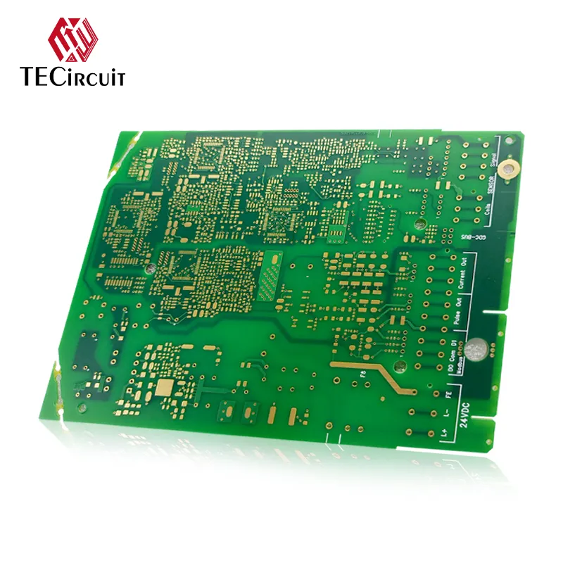
In the technology sector, accuracy and optimization go together with innovation. When it comes to printed circuit boards (PCBs), the backbone of contemporary electronics, effectiveness isn't just a goal-- it's an one-upmanship. Stiff PCBs, where components are electrically interconnected on rigid substrates, go to the forefront of this effectiveness drive, requiring next-gen design techniques to fulfill the expanding needs of high-speed applications. Here, we check out some sophisticated style considerations and best techniques in inflexible PCB format.
Maximizing PCB Design for Heat Administration
Warmth dissipation is an essential consideration in the long life and security of digital gadgets. Inflexible PCBs with inadequate warmth monitoring can cause parts overheating, lowering their functional life and the overall security of the device. A correct format that includes the strategic positioning of thermally conductive traces, thermal vias, and warmth sinks can substantially enhance the board's capacity to handle thermal lots.
Including huge copper pours and power aircrafts, as well as a sensible spacing of parts to allow airflow, are reliable design strategies. Furthermore, using component thermal pads and taking into consideration the orientation of the board within the device or room can assist in natural convection cooling. A maximized layout additionally introduces the concept of thermal resistance in early stages, making certain that the heat generated by crucial parts is successfully carried away from the critical areas.
The Value of Layer Stack-Up Arrangement in RIGID PCBs
The stack-up arrangement influences the electric performance and signal honesty of a PCB. It defines the placement of power and ground aircrafts, signal layers, and dielectric products, which play a significant duty in regulating resistance, crosstalk, and RF disturbance.
A well-structured stack-up commonly includes high-speed signal layers sandwiched in between power and ground aircrafts to give constant reference airplanes for signal return courses. Differential pair transmitting and regulated insusceptibility tracks can be accomplished better when the right layer stack-up is used. For stiff boards, lessening the range in between layers can cause minimized layer-to-layer shift results, which are essential for preserving signal stability in high-frequency applications.
Signal Stability Obstacles in High-Speed PCB Designs
In the world of high-speed PCBs, making sure signal honesty (SI) is critical. Poor SI can lead to information corruption, performance degradation, and the demand for pricey redesigns. Impedance matching, trace length tuning, and lowering alter are typical techniques for SI, but they call for thorough focus to information.
Devices like field solvers and simulation software application can aid in evaluating SI features throughout the style phase. They help in predicting and attending to issues such as representations and timing mismatches that can take place at interfaces and adapters. With flexible pcb coming to be a lot more widespread, the need for strenuous SI evaluation and layout validation approaches has actually never been extra critical.
Making Use Of Embedded Components in RIGID PCBs for Room Conserving
To address the miniaturization pattern in consumer electronics, inflexible PCBs now commonly consist of ingrained elements innovation (ECT). ECT involves embedding easy components-- like resistors, capacitors, and inductors-- directly into the PCB substrate, which not only minimizes the board's footprint but also minimizes parasitics and boosts signal performance.
Embedding parts also improves the board's mechanical toughness and reliability by protecting the parts from environmental variables. However, it calls for a cautious evaluation of the mechanical and thermal buildings of the embedded materials to make certain that they do not influence the board's honesty or the efficiency of other components.
Ideal Practices for Multi-Layer RIGID PCB Layout
Multi-layer Stiff PCBs are the go-to option for complex and high-density layouts. Taking care of power circulation, controlling insusceptibility, and keeping an excellent ground framework are key locations for problem in multi-layer layouts. Partitioning the PCB right into power, ground, and signal areas, and utilizing correct decoupling techniques, can assist distribute power effectively and minimize noise on the power rails.
Making sure symmetry in the layer stack-up is essential for maintaining controlled impedance, specifically for differential pairs. Additionally, managing crosstalk by maintaining the appropriate spacing and using guard traces can significantly improve signal high quality. It's also vital to utilize design policies that enable for very easy manufacturing and testing, such as keeping appropriate clearances and remaining within the manufacturer's specs for minimal function dimensions.
In https://tecircuit.com.cn/products/ , STIFF PCB design is a complex process that includes maneuvering numerous design restrictions, part positioning, and layer stack-ups to accomplish optimum electric performance, mechanical integrity, and thermal monitoring. By using the most recent style methodologies and considering the full lifecycle of the product, designers can produce PCBs that not just function dependably yet additionally add to the general performance and robustness of the last gadget.